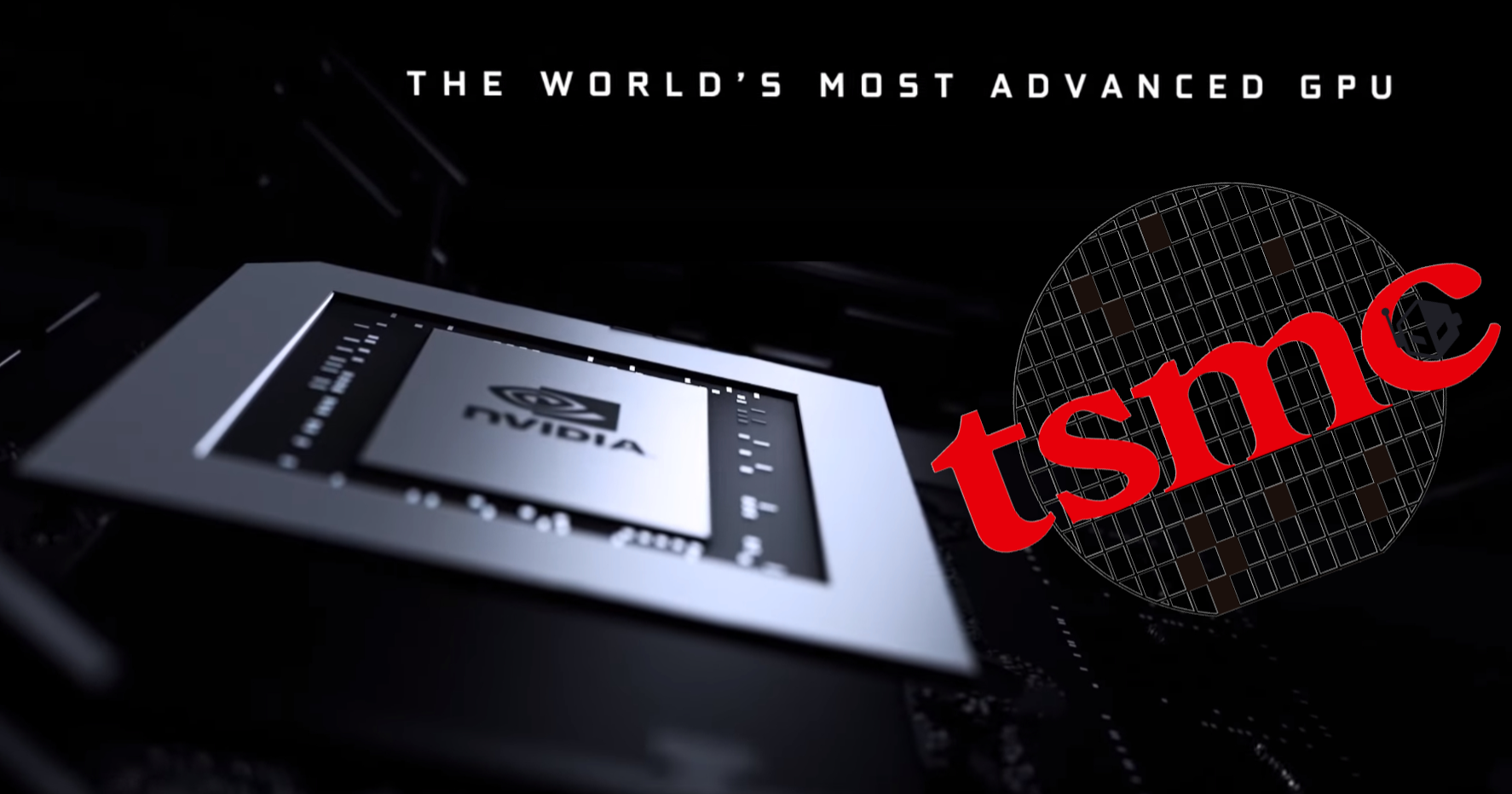
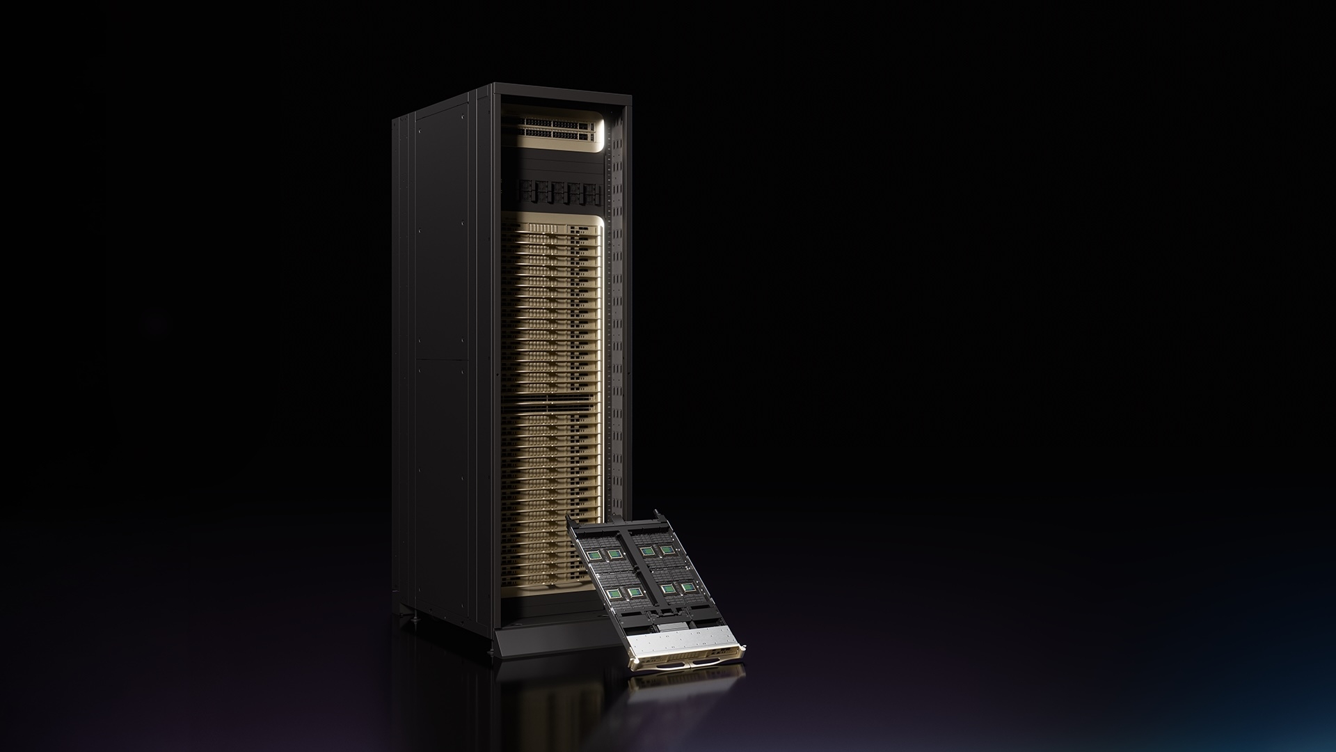
Semiconductor design and manufacturing are about to enter a new era of precision, thanks to a collaboration between two industry giants. NVIDIA’s AI expertise is being paired with TSMC’s advanced fabrication capabilities, creating a pipeline that could redefine how chips are built—from the ground up.
The focus isn’t just on speed or scale; it’s on embedding intelligence into every stage of production. This shift could mean shorter development cycles for next-generation processors and more efficient use of silicon resources, both critical factors as demand for AI-accelerated hardware continues to grow.
Why This Matters
The collaboration centers on two key areas: design optimization and manufacturing efficiency. On the design side, NVIDIA’s software tools will leverage AI to refine semiconductor layouts with unprecedented accuracy. This could translate into chips that perform better while consuming less power—a balance that’s become increasingly important for data center workloads.
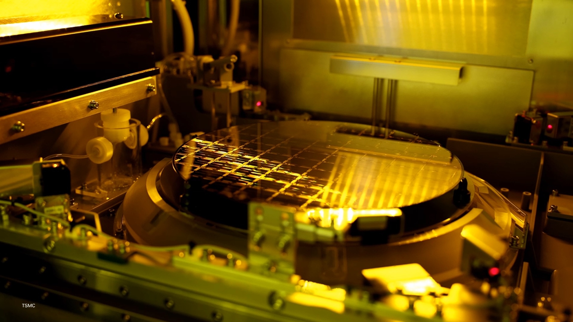
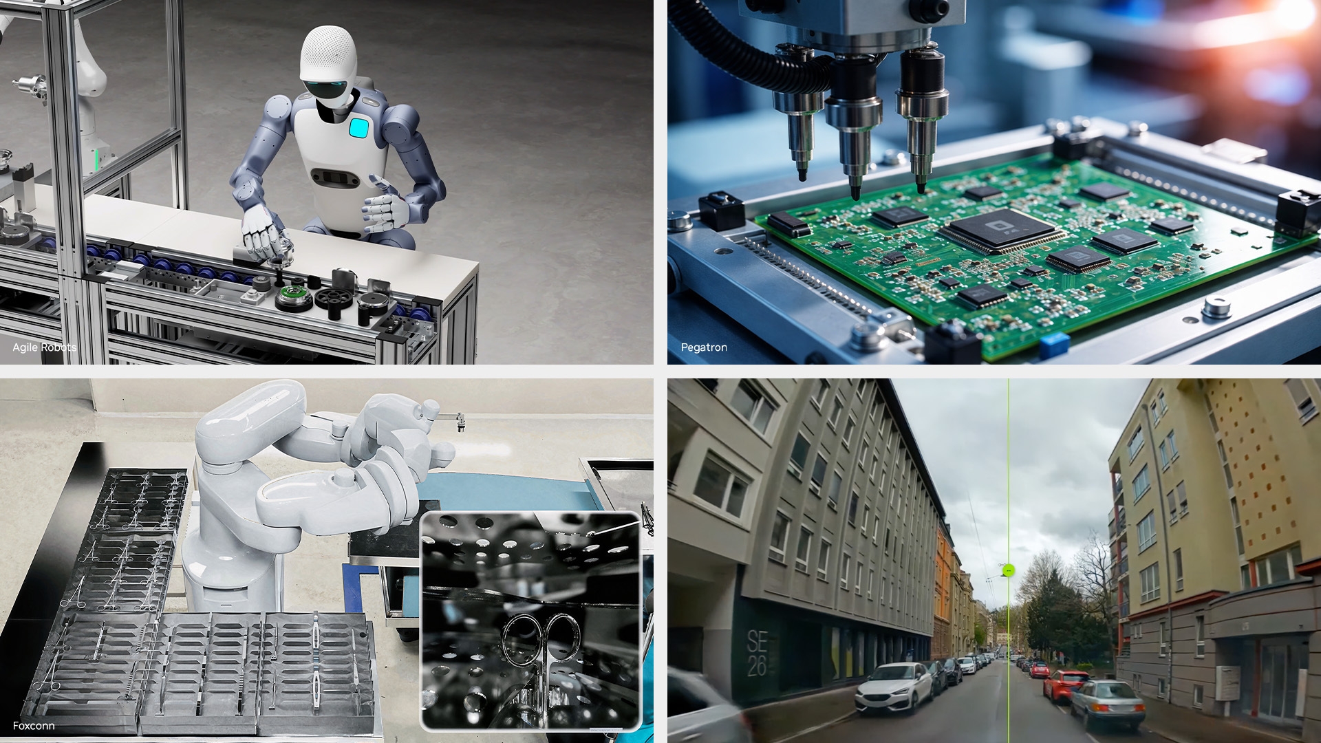
Simultaneously, TSMC is integrating AI-driven process control into its fabrication plants. The goal? To reduce defects and improve yield without sacrificing performance. Early indicators suggest this approach could cut production times by as much as 30% in some scenarios, though exact figures will depend on real-world implementation.
What’s Next
For now, the partnership is still in its early stages, with no specific products or timelines announced. However, the implications for the industry are clear: AI is moving from the data center to the factory floor, and the chips that power tomorrow’s applications could be built smarter than ever before.
The biggest question remains whether this collaboration can translate theoretical gains into tangible improvements without disrupting existing supply chains. If successful, it could set a new standard for semiconductor innovation—one where intelligence isn’t just a feature of the chip, but a fundamental part of how it’s made.