Tesla’s TeraFab project has evolved from a speculative idea into a hardware-first strategy, with Musk explicitly targeting 3nm and 2nm process nodes—a leap that would position Tesla among the most advanced foundries globally. The facility’s design now includes dedicated memory production, a rare capability even among legacy players like Micron and SK Hynix, suggesting Tesla intends to eliminate external dependencies entirely.
The 100–200 billion chips per year target isn’t just about volume—it’s about cost per wafer. At scale, Tesla could undercut foundries on pricing, particularly for its proprietary silicon like the AI5 and future AI9 chips. Industry insiders note that even TSMC’s most efficient fabs produce ~10–15 billion wafers annually, meaning Tesla’s goal would require 10x the output of its largest competitor.
Talent and tech are the wild cards. Recruiting 3nm/2nm engineers—many of whom work at TSMC, Samsung, or Intel—will be a Herculean task. The equipment alone, including extreme ultraviolet (EUV) lithography tools, costs billions per installation, and Tesla would need to secure multiple systems to meet its timeline. Musk has hinted at partnerships with ASML and Applied Materials, but no formal agreements have been announced.
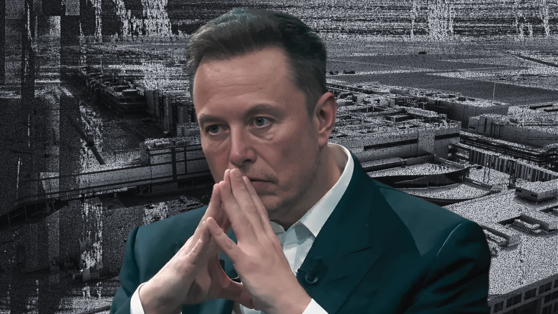
What’s next? Construction on TeraFab’s first phase is underway in Austin, with early production targeting 5nm and 4nm nodes by 2025. If successful, Tesla could vertically integrate its entire silicon supply chain—from design to packaging—by 2028. The real test? Whether the company can bridge the 3nm gap without decades of R&D experience. For now, the industry watches, skeptical but intrigued by the disruption.