Intel's push into the 14A node represents a critical turning point for the company's manufacturing strategy. While the 18A node faced notable challenges, the 14A node is advancing more smoothly, promising improved yields and a streamlined production process. This shift is not just about internal gains; it also positions Intel to compete more effectively in the foundry space against established players like TSMC.
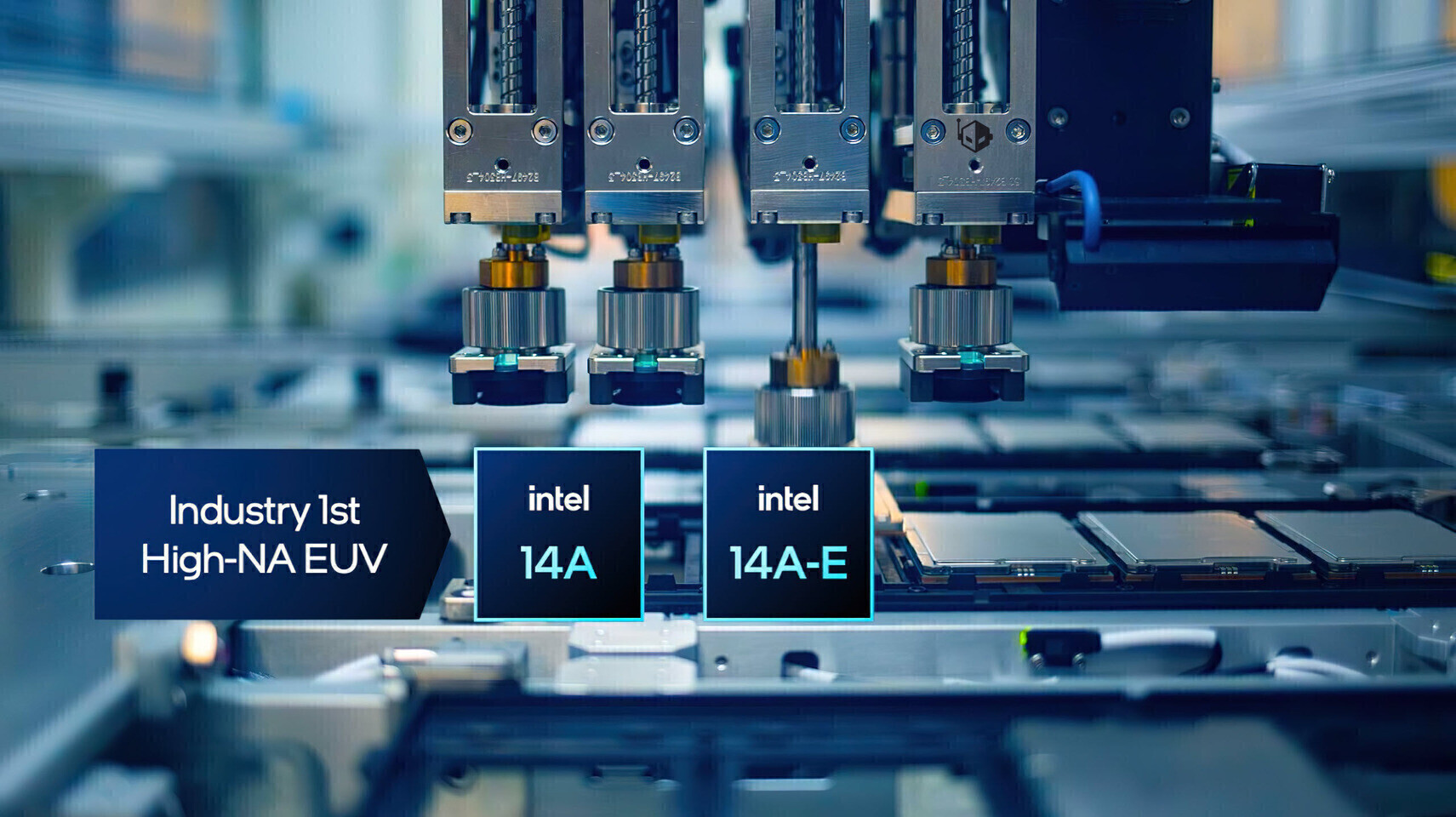
One of the most significant aspects of this development is the integration of ASML's High-NA EUV lithography tools. These tools, already a staple in advanced semiconductor manufacturing, are being utilized for the first time globally at this node. This move underscores Intel's commitment to staying at the forefront of technological innovation, even as it navigates the complexities of scaling down to smaller nodes.
Key Specifications and Timeline
- Node: 14A
- Risk Production Start: 2028
- High-Volume Manufacturing: 2029
- EUV Tools: ASML High-NA EUV lithography
The 14A node is currently at the 0.5 PDK stage, with a significant milestone expected in October of this year when the 0.9 PDK will be released. This 'holy grail' as Intel CEO Lip-Bu Tan refers to it, will allow customers to begin their designs, marking a crucial step in the node's development lifecycle.
Competitive Landscape and Future Nodes
Intel is not only focusing on its own advancements but also on positioning itself as a viable alternative to TSMC. The 14A node is seen as a direct competitor to TSMC's A14 node, which is expected to enter the market around the same time. This competition will likely drive further innovation and efficiency in semiconductor manufacturing processes.
Looking ahead, Intel has hinted at adding more nodes to its roadmap, specifically the 10A and 7A nodes. These future developments aim to build a continuous evolution of technology, catering both to internal needs and customer commitments. The goal is to create a long-term plan that attracts customers in the same way TSMC does, offering a framework for future node exploration.
The 14A node's risk production in 2028 and high-volume manufacturing in 2029 will coincide with major customers ramping up their designs. Intel plans to utilize this node both internally and offer it to third-party customers, who will consume High-NA EUV exposed wafers at scale. This dual approach ensures that Intel remains a key player in the semiconductor industry, balancing internal innovation with external market demands.
While the 14A node represents a significant step forward, there are still uncertainties and challenges ahead. The success of this node will depend on various factors, including yield improvements, production efficiency, and market adoption. Intel's ability to navigate these complexities will be crucial in determining its long-term success in the competitive semiconductor landscape.
In summary, Intel's 14A node is a pivotal development that could redefine the company's trajectory in semiconductor manufacturing. With a focus on innovation, efficiency, and long-term customer commitments, Intel aims to solidify its position as a leader in this critical industry segment. The roadmap for the 10A and 7A nodes further underscores this ambition, setting the stage for a continuous evolution of technology that could shape the future of computing.