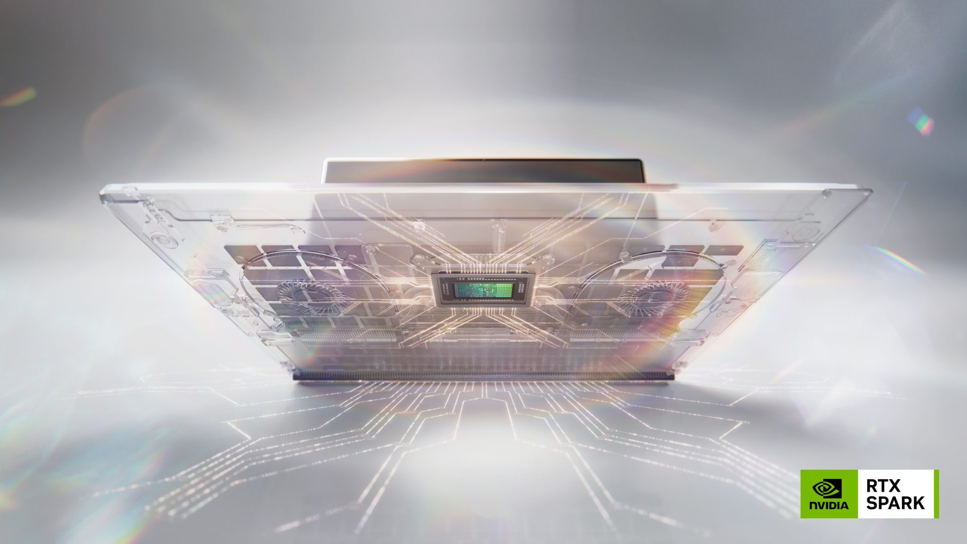
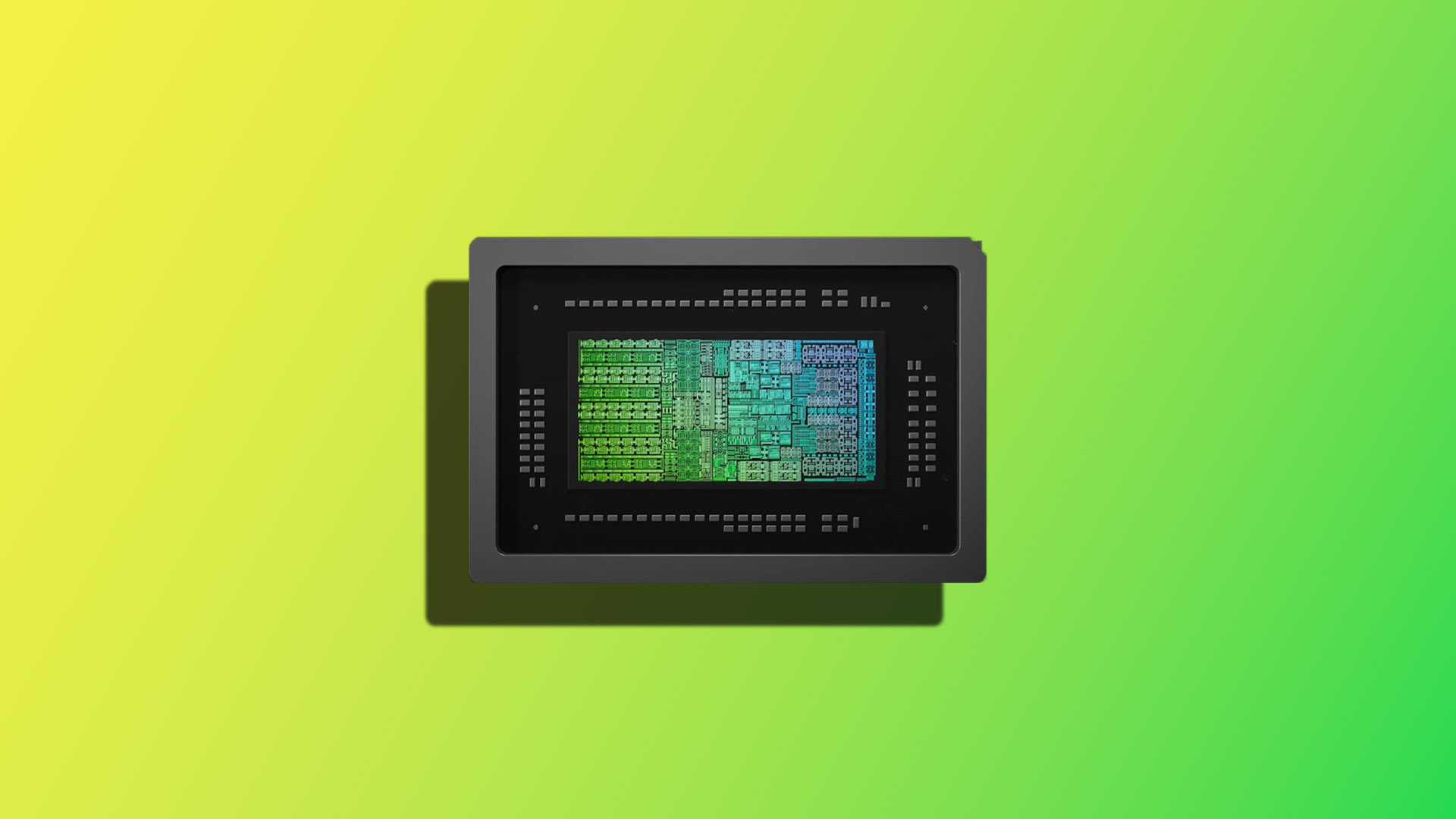
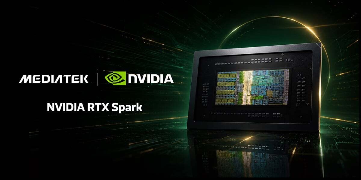
Analysis Computex 2026 Hardware NVIDIA’s RTX Spark Is a Direct Shot at the PC Market, Backed by a Multi-Gen Roadmap That Past ‘Windows on Arm’ Bids Never Had Hassan Mujtaba • at EDT Add on Google NVIDIA has announced RTX Spark, its brand-new PC platform, designed in collaboration with Microsoft, as it starts a new chapter of its client brand. NVIDIA RTX Spark May Look Like The Standard AI SoC Affair For PCs, But It's Much Bigger Than That Today at GTC Taipei 2026, a conference hosted by NVIDIA and presented by CEO Jensen Huang, the company unveiled its brand new chip for the PC segment, which they are calling RTX Spark. According to NVIDIA, the RTX Spark reinvents the PC. This project was initiated three years ago with Microsoft, Arm, MediaTek, and other ecosystem partners. Related Story MSI Pushes NVIDIA’s RTX Spark Into The Mainstream With A Developer Mini PC And A Tandem OLED Flip Laptop Last year, NVIDIA introduced the DGX Spark. The DGX Spark was designed as an AI-first machine, with 128 GB of LPDDR5X memory, the Grace CPU core, and Blackwell GPU architecture. It's like NVIDIA taking its Grace Blackwell datacenter GPUs and optimizing a configuration that is suitable for small and more accessible form factors. The RTX Spark builds upon DGX Spark's GB10 Superchip, which is also internally referred to as N1X, with a lighter configuration called N1. These SoCs are called DGX Spark for the AI, & RTX Spark for the client platforms. RTX Spark Specs Deep-Dive So let's start with the specifications first. NVIDIA's RTX Spark SoC is very much a GB10 Superchip that combines the two aforementioned architectures through Connect-X. NVIDIA developed the GB10 Superchip, which combines innovations from datacenters, such as NVFP4, CUDA, SLANG, TensorRT, vLLM, CX-7 NIC, NVLINK C2C, TMEM, and more, down to client platforms that utilize a smaller form factor, made possible using multi-die packaging tech, a very low-power C2C interface, and Unified Memory Architecture (UMA). As a result, the DGX Spark Workstation was built, which offers the following key features and benefits: GB10 Grace Blackwell Superchip: Accelerates AI, Data Science, Compute, Rendering & Visualization 128GB Coherent Unified System Memory: Works with Large AI models up to 200 billion parameters, fine-tune models of up to 70 billion parameters ConnectX-7 Networking: Connect two DGX Spark systems to work with models of up to 405b parameters DGX Base OS and NVIDIA AI Software Stack: Seamlessly move workloads from DGX Spark to DGX Cloud or any accelerated data center or cloud infrastructure Flexible deployment configurations: Configure as an AI Workstation or a network-connected personal AI cloud Great Desktop Experience: Multi-head display support and flexible connectivity Compact, power-efficient design: Easily fits on any desk, powered by a standard wall outlet So let's dive into the specifications of the GB10 Superchip. First up, we have the SoC composition, which shows that the chip itself is composed of two dielets, an S-Dielet which houses the CPU, memory subsystem, etc, and a G-Dielet which houses the GPU core. These two dielets are packaged together using Advanced 2.5D packaging and are fabricated on TSMC's 3nm process technology. The CPU is based on the ARM Arch v9.2 architecture with 20 cores, custom-designed by MediaTek. There are 2 clusters of 10 cores each, and each core has a private L2 cache and a 16 MB L3 cache per cluster, so 32 MB in total. The GPU is based on the GB100 Blackwell architecture and is considered an iGPU since it is on the same package and silicon. It features 5th Gen Tensor Cores with DLSS, Reflex, ACE, G-Sync, REFLEX, CUDA, NVFP4 support, and RTX Ray Tracing cores. It produces up to 31 TFLOPs of FP32 and 1000 TOPS of NVFP4 (FP4) compute for AI workloads. The GPU also gets an additional 24 MB of L2 cache. Moving into the memory system, the NVIDIA GB10 Superchip SOC features support for 256b LPDDR5x (UMA) with up to 9400 MT/s speeds, enabling up to 301 GB/s of raw bandwidth, and up to 128 GB of maximum capacities. The system fabric is a high-performance coherent fabric that offers support for CHI-E Coherency Protocol. The GPU has access to the entire system bandwidth of 600 GB/s (Aggregate) over the C2X interface. NVIDIA will allow the unified memory pool to be allocated manually to the GPU. A 128 GB system can dedicate up to 111 GB of system memory to the GPU without opening the UEFI BIOS; it will be done directly through Windows. There's also 16 MB of System Level Cache, which serves as L4 for the CPU, and enables power-efficient data-sharing between the multiple engines on the SoC. The C2C interface is also high-bandwidth and low-power, enabled through NVIDIA's NVLINK architecture. On the connectivity side, NVIDIA's GB10 Superchip SoC offers PCIe, USB, Ethernet over PCIe, and drives up to 4 concurrent displays (3 DP + 1 HDMI) at up to 4K @120Hz with DP Alt-mode, and up to 8K @ 120Hz with HDMI 2.1a. Security features include Dual Secure Root support, SROOT processor, OSROOT processor, and support for both fTPM and discrete TPM. The whole chip has a TDP of 140W. Following is the block diagram of the NVIDIA GB10 Superchip SoC: Scalability is also another fun aspect of the GB10 Superchip. You can connect multiple GB10 chips through NVIDIA's ConnectX Technology and scale throughput, bandwidth, and DRAM capacities to support larger AI models. The ConnectX NIC is connected to the GB10 SoC using a PCIe Gen5 x8 interface, and the units communicate with each other using Ethernet. The Software Enablement & Early Previews Why I say that NVIDIA has a better chance than others in crunching away client PC market share from x86 giants such as Intel and AMD is because, unlike Snapdragon X1 and X2 series, which were a first attempt by Qualcomm on the PC, NVIDIA has a full-fledged and optimized framework around Windows. The answer is simply: RTX. NVIDIA's RTX platforms have already been powering desktops and laptops. The company has a very solid driver support, and its Linux support has also improved substantially, with DGX Spark systems seeing some big updates. TensorRT and CUDA support remain great on Windows, & that gives NVIDIA a better chance at the "WoA" segment than what others have tried in the past. One of the biggest challenges for NVIDIA won't be the GPU, but the CPU. Grace currently remains entirely untested as a Windows chip. The benchmarks that have been floating around for more than a year are all DGX-based through emulation or on Linux. During our technical sessions with the GeForce Team, we saw games and applications such as Blender, Unreal Engine, LLM Studio, OpenClaw, and many more running at reasonably fast performance. In closed testing done by NVIDIA, the chip was getting up to 10x faster AI performance, and up to 2x faster GenAI performance. The gaming performance in titles such as Alan Wake II, Fortnite, and Indiana Jones was great too. But the numbers have to be taken with a grain of salt, and NVIDIA isn't providing any FPS figures, nor showing the settings used to run these games. Though we were told that the games were running with DLSS Frame-Gen enabled. RTX Spark, being based on the Blackwell IP, means that it will support all innovations such as DLSS 4.5 Ray Reconstruction, Multi-Frame Gen, and much more. NVIDIA is also working with various partners, including the XBOX Team and Krafton, to bring next-gen experiences to RTX Spark. A Multi-Generational Plan The key to success for any platform is to make a statement that it won't just end after one launch. For RTX Spark, NVIDIA fully commits to the PC platform, & offered a look into what comes after the first-gen RTX Spark systems. In the first generation, NVIDIA RTX Spark systems will combine the Grace CPU & Blackwell GPU with LP5X memory. These will be available in the fall of 2026. The next chapter of RTX Spark will arrive by 2028, offering Vera CPU and Rubin GPU arc...