For decades, the evolution of semiconductors has been a story of shrinking transistors. Now, as AI-driven data centers demand ever-larger, more complex chips, Kyocera is taking a different approach: building the foundation beneath those chips from ceramic instead of organic materials.
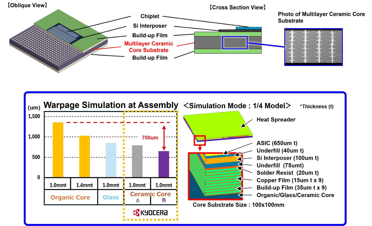
The company’s new multilayer ceramic core substrate promises to address two critical bottlenecks in high-performance semiconductor packaging—warpage and wiring density. While traditional organic substrates struggle with deformation under heat and mechanical stress, Kyocera’s design leverages its proprietary Fine Ceramic technology to deliver a rigid structure that resists bending, even at scale. This rigidity is crucial for 2.5D packaging architectures, where multiple layers of silicon must align precisely without warping.
Why Ceramic? The Shift from Organic Substrates
The push toward ceramic isn’t just about stability; it’s also about precision. Conventional organic substrates rely on drilling to create vias—the conductive paths between layers—but this method limits how fine those connections can be. Kyocera’s process, which shapes vias while the ceramic is still pliable before firing, allows for smaller diameters and tighter pitches. The result? Higher wiring density without sacrificing reliability.
- Reduced Warpage: Ceramic substrates maintain their shape under thermal cycling, a common issue in large packages where organic materials can bend or twist over time.
- Finer Wiring: Microfabrication techniques enable vias as small as 10 micrometers in diameter, compared to the 20–30 micrometer limits of drilled organic substrates.
- Custom Design Support: Kyocera offers thermal and electrical simulations during the design phase, helping manufacturers optimize performance before production begins.
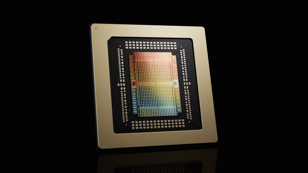
This shift matters most for next-generation xPUs (accelerator processing units) and ASICs (application-specific integrated circuits), which are becoming the backbone of AI data centers. As these chips grow in complexity—some now exceeding 1,000 square millimeters—their packages must keep up without introducing defects or performance degradation.
From Lab to Market: The Road to Commercialization
The new substrate will be unveiled at the Electronic Components and Technology Conference (ECTC) in Orlando later this month, marking Kyocera’s latest contribution to semiconductor packaging innovation. While competitors like Broadcom have already demonstrated 2 nm custom compute chips built on 3.5D platforms, Kyocera’s focus on ceramic core substrates addresses a different layer of the challenge: the physical substrate itself.
For buyers, the practical implication is clearer efficiency and longevity in AI infrastructure. A data center operator using these substrates could expect fewer defects during manufacturing and more stable performance over time—critical factors as chip sizes push beyond traditional limits. Yet, adoption won’t be instantaneous; cost remains a barrier, and not all foundries may transition to ceramic immediately.
The broader trend is clear: as AI accelerates demand for larger, denser chips, the materials beneath them must evolve just as rapidly. Kyocera’s substrate is one piece of that puzzle, proving that sometimes, going back to basics—like using ceramic instead of organic layers—can unlock the next frontier.