TSMC has accelerated the commercial rollout of its CoPoS packaging, a direct replacement for legacy CoWoS that uses glass core substrates. The shift could cut manufacturing costs by nearly one-third and boost wafer efficiency to over 90%, but not all chip designs will benefit equally.
The technology, which stacks dies on a glass interposer, addresses two persistent pain points in advanced packaging: cost per unit and fabrication waste. By eliminating the need for organic substrates, TSMC reduces material expenses while increasing the number of functional chips that can be produced from a single wafer. However, the practical impact hinges on whether high-performance designs—particularly those relying on dense signal routing—can adapt without performance degradation.
Performance trade-offs in practice
The 30% cost reduction is achieved through a combination of material savings and higher wafer utilization. Where CoWoS typically yields around 85-90% efficiency, CoPoS pushes that figure past 90%, meaning fewer defects per wafer. For power users, the immediate benefit is clearer pricing tiers for high-end packages, but the trade-off lies in thermal management: glass substrates conduct heat less efficiently than traditional organic materials.
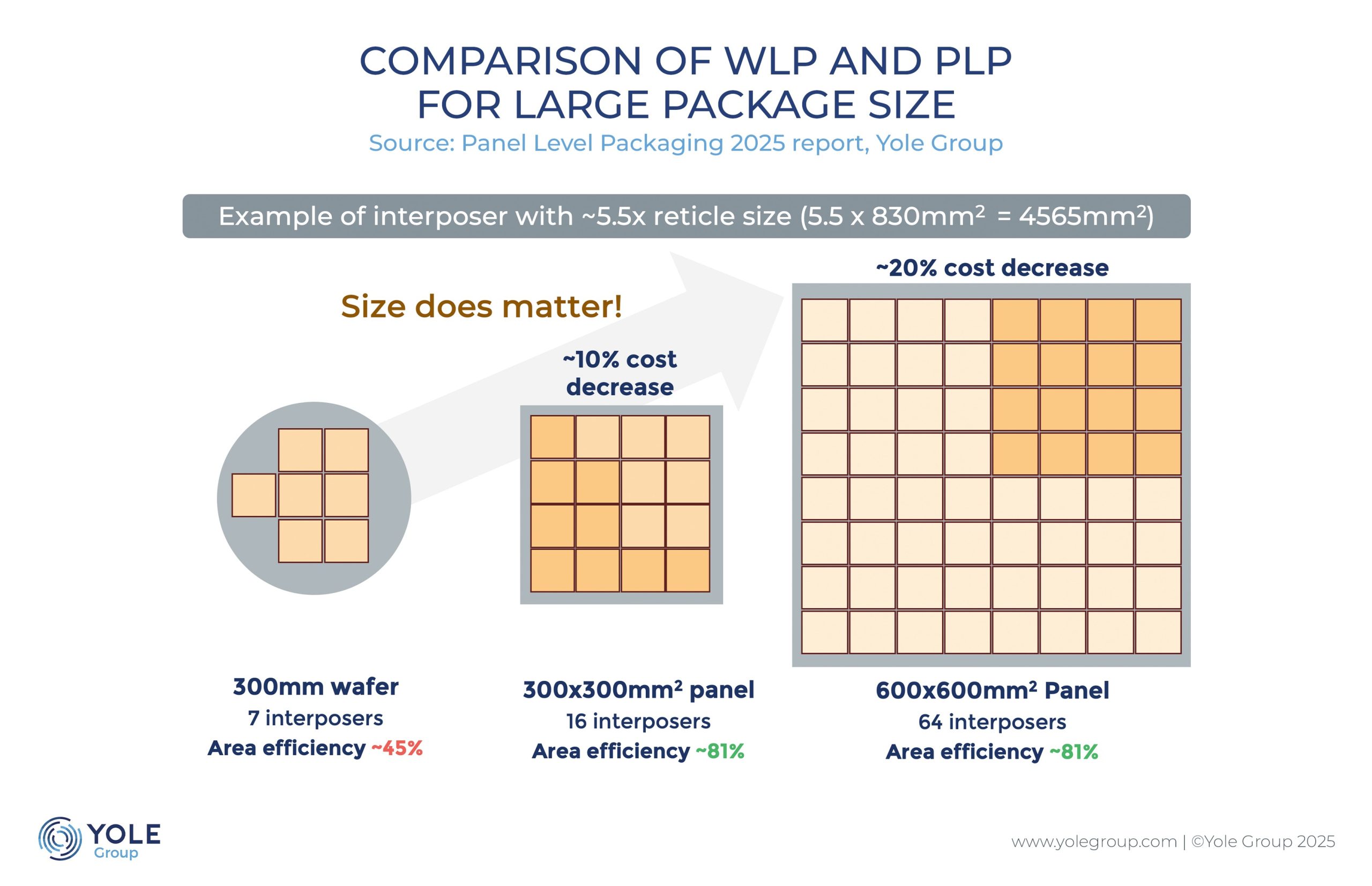
- Up to 30% lower cost through material and process optimizations
- Wafer utilization jumps from ~90% to over 90%
- Glass interposer enables finer pitch routing but with thermal constraints
Compatibility risks for next-gen designs
The glass substrate introduces a fundamental constraint: signal integrity can degrade in high-speed interconnects if routing density isn't carefully managed. TSMC has addressed this in its reference implementations by optimizing bond pad placement, but custom designs may still require re-architecting to avoid bottlenecks. This is where the economic advantage could turn into a compatibility risk—especially for AI accelerators or GPUs that demand ultra-low latency.
For end users, the day-to-day impact will be most noticeable in mid-range products, where price sensitivity often outweighs performance margins. High-end applications, however, may see only incremental gains unless TSMC can prove long-term stability under heavy thermal loads.
What's confirmed vs. what remains uncertain
The 30% cost reduction and >90% wafer utilization are backed by internal benchmarks, but real-world adoption depends on two unknowns: first, how quickly foundries outside TSMC adopt the technology; second, whether thermal limitations will force design compromises in next-generation chips. If both are resolved, CoPoS could become the default for mid-tier packages within 18 months.
Investors should watch this space closely—those betting on cost-sensitive segments like smartphones or entry-level GPUs stand to gain the most, while high-performance markets may need to wait for a second-generation refinement. The technology's success hinges not just on its technical merits but on how effectively TSMC can navigate these trade-offs and adapt it to evolving design requirements.