Tesla’s Ambitious Expansion: The ‘TeraFab’ Project
Tesla is pursuing a multifaceted strategy aimed at bolstering its supply chain control, particularly regarding specialized semiconductors. This initiative centers around the construction of a network of advanced fabrication facilities, dubbed ‘TeraFabs,’ designed to produce custom chips tailored to Tesla's needs – including those powering its burgeoning AI initiatives.
The 2nm Target: A Significant Leap
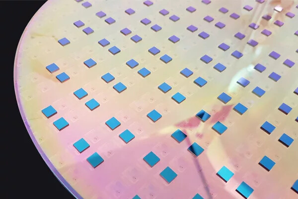
Initial announcements regarding the TeraFab project outlined ambitions for manufacturing at a 5nm node. However, recent statements from Elon Musk indicate a substantial scaling up of this goal. He has publicly stated Tesla intends to build facilities capable of producing chips at a 2nm process technology. Achieving such a fine feature size represents a considerable technological challenge, demanding significant investment in equipment and expertise. The move underscores Tesla’s long-term commitment to self-sufficiency in critical semiconductor production.
Cleanroom Controversy: A Rejection of Established Practices
Perhaps the most surprising element of Musk's recent is his apparent dismissal of conventional cleanroom environments within the TeraFab facilities. During discussions, he suggested that he could be routinely observed inside the fabrication plants with a cigar. This statement has ignited considerable debate and raised fundamental questions about how Tesla envisions managing the stringent environmental controls required for advanced chip manufacturing.
Why Cleanrooms Matter: A Technical Overview
Cleanrooms are meticulously controlled environments designed to minimize particulate contamination – dust, fibers, aerosols, and other airborne contaminants. These particles can drastically impact semiconductor fabrication processes, leading to defects in the chips being produced. The 2nm node, in particular, demands an exceptionally high level of cleanliness, necessitating sophisticated air filtration systems, specialized materials, and rigorous protocols to prevent even trace amounts of contamination. Traditional cleanroom design focuses on maintaining a specific pressure differential and controlled airflow to capture and remove airborne particles.
Tesla’s Reasoning (Speculative): Cost and Speed Optimization
While Musk hasn't explicitly detailed his rationale, several factors could contribute to this unconventional approach. A key consideration is likely cost – cleanroom construction and operation are notoriously expensive. Tesla may be prioritizing speed of deployment and potentially lower capital expenditure by foregoing traditional cleanroom setups. Another factor could be a focus on process optimization, where tighter control over the environment isn't deemed as critical at this initial stage of development.
Samsung Foundry Collaboration: A Strategic Partnership
It’s important to note that Tesla's chip ambitions aren’t solely reliant on its internal TeraFab network. The company has forged a significant collaboration with Samsung Foundry for the production of AI5 and AI6 chips. This partnership leverages Samsung’s established expertise in advanced semiconductor manufacturing while allowing Tesla to access cutting-edge fabrication capabilities without undertaking the massive capital investment required to build its own facilities from scratch. This strategic alliance seems designed to provide a phased approach to chip development, starting with leveraging external partners and eventually incorporating internally produced components.
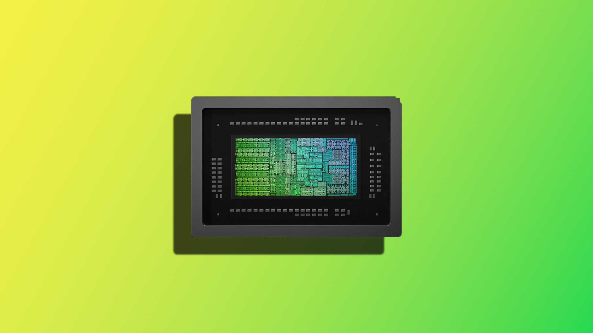
The AI5 & AI6 Chips: Powering Tesla’s Future
The AI5 and AI6 chips are central to Tesla's autonomous driving capabilities and its broader push into artificial intelligence. These specialized processors demand high performance and efficiency, making them ideal candidates for in-house fabrication – a goal that the TeraFab project aims to achieve. Details regarding the specific architectures and features of these chips remain largely confidential, but their development is undoubtedly a key driver behind Tesla's ambitious manufacturing plans.
Potential Implications and Challenges
Tesla’s approach to chip fabrication presents several potential implications for the broader semiconductor industry. If successful, it could disrupt traditional foundry models, potentially leading to increased competition and lower chip prices. However, the challenges are equally significant. Manufacturing at 2nm is a formidable undertaking requiring considerable technological expertise and substantial investment. Maintaining quality control without established cleanroom protocols poses a major risk.
Looking Ahead: A Bold Gamble
Tesla’s ‘TeraFab’ project represents a bold gamble – one that could fundamentally reshape the landscape of semiconductor manufacturing. The company's willingness to challenge conventional wisdom and prioritize speed and cost over established practices will be closely watched by industry observers. Whether Tesla can successfully execute its ambitious vision remains to be seen, but its pursuit underscores the growing demand for greater supply chain control and self-sufficiency within the automotive and technology sectors.