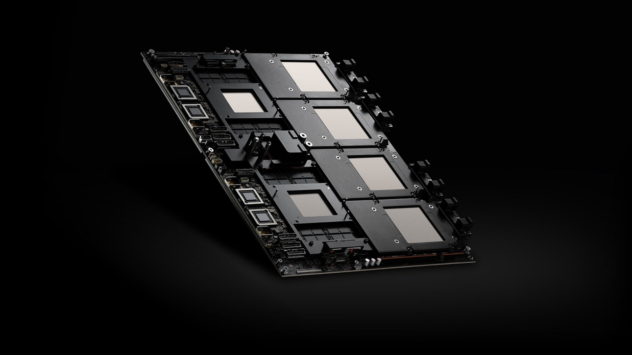
A breakthrough in semiconductor packaging has arrived with the launch of two advanced interconnect process design kits (PDKs) by the NanoIC pilot line. These tools, designed for high-density chip-to-chip connections, represent a major step forward in enabling more efficient and powerful system-on-chip designs beyond the 2 nm node.
Traditional packaging methods have struggled to keep pace with the demands of modern computing, particularly in areas like AI accelerators and high-performance GPUs. The new PDKs—one for fine-pitch redistribution layer (RDL) and another for die-to-wafer (D2W) hybrid bonding—address this gap by introducing polymer-based substrates with ultra-fine interconnects and oxide-to-oxide bonding techniques. These innovations promise to reduce energy consumption per bit while increasing communication speed, making them ideal for next-generation architectures.
Advanced Packaging for Next-Gen Systems
The fine-pitch RDL PDK achieves line widths as small as 1.3 microns and microbump pitches down to 20 microns, enabling up to a 40% improvement in communication speed and a 15% reduction in energy per bit when used with UCIe-Advanced interfaces. Meanwhile, the D2W hybrid bonding PDK eliminates parasitic losses from copper bumps, creating low-latency pathways that are particularly valuable for AI workloads and high-bandwidth computing.

Practical Impact on Design and Efficiency
For IT teams and developers working on advanced chip designs, these PDKs offer immediate practical benefits. The fine-pitch RDL allows for more compact, energy-efficient routing on polymer substrates, which is crucial for applications like automotive systems and next-gen GPUs. At the same time, D2W hybrid bonding provides ultra-dense 3D connections that can significantly enhance bandwidth and performance in AI accelerators.
What sets these PDKs apart is their accessibility—designed to be used by universities, startups, and industry players, they provide early access to cutting-edge interconnect technologies. As the tools mature, they will evolve into full tape-out capabilities, allowing designers to transition from simulation to real silicon validation.
Looking ahead, the introduction of these PDKs signals a shift toward more integrated, high-density chip designs. For organizations focused on efficiency and performance, this represents a critical opportunity to push the boundaries of what’s possible in advanced computing and AI systems.