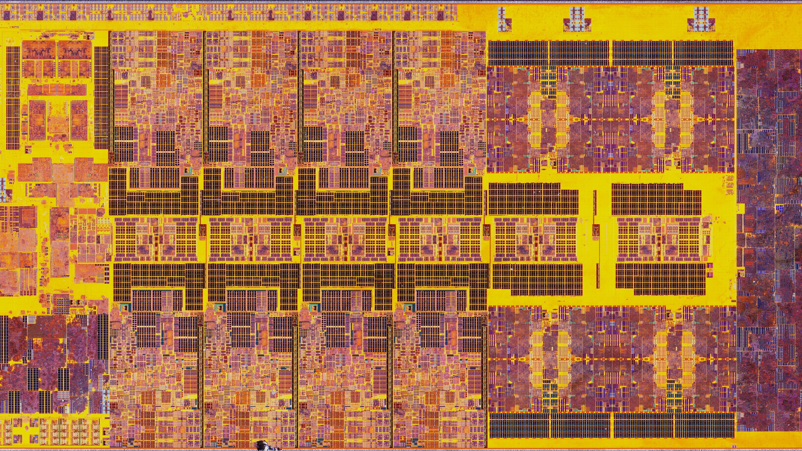
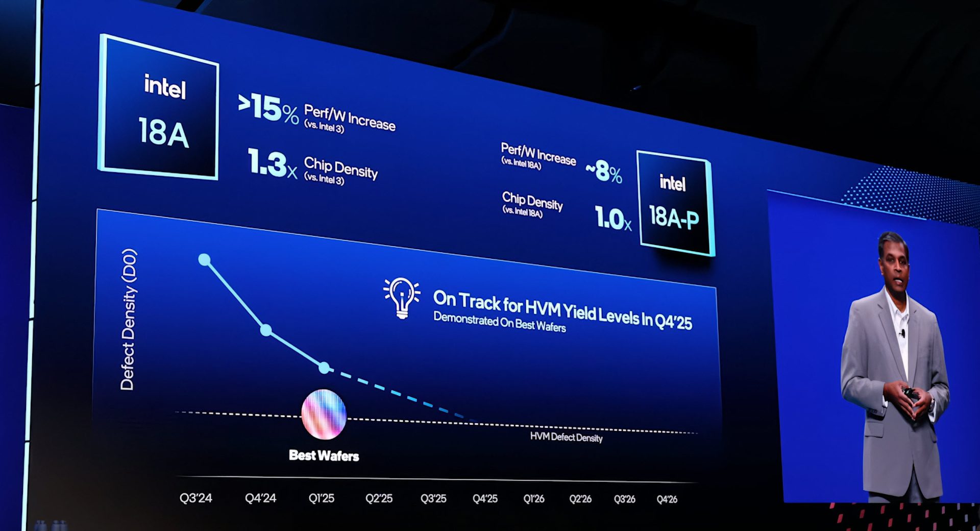
Intel’s 18A-P process node has emerged as a critical milestone in semiconductor manufacturing, drawing significant attention from industry giants. This advanced process, designed for high-performance chips, is now being adopted by Apple and Google, marking a strategic shift that could reshape the competitive landscape.
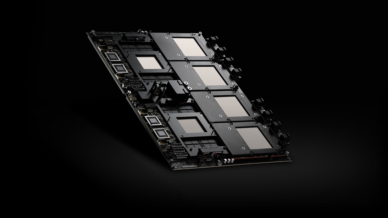
The 18A-P node, part of Intel’s roadmap for next-generation processors, offers improvements in power efficiency and performance. Its adoption by Apple suggests a move away from traditional foundry models, signaling a stronger integration between design and manufacturing. Meanwhile, Google’s reported interest in EMIB (Embedded Multi-die Interconnect Bridge) technology further highlights the growing demand for advanced packaging solutions.
For power users and tech enthusiasts, this development is notable for several reasons. First, it indicates that Intel is regaining ground in high-performance chip manufacturing, a sector where it has historically faced challenges. Second, the shift toward advanced packaging like EMIB suggests a more modular approach to chip design, which could lead to more flexible and efficient hardware solutions.
Intel’s 18A-P process node is expected to support a wide range of applications, from mobile devices to data center workloads. Its adoption by major players like Apple and Google underscores the importance of this technology in driving future innovation. As the industry continues to evolve, Intel’s ability to deliver on its promises will be closely watched.