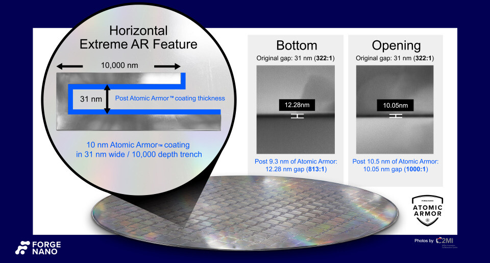
Thursday, February 5th 2026 Forge Nano Transforms Advanced Semiconductor Chip Manufacturing with High-Speed 1000:1 Aspect Ratio Atomic Layer Deposition Coatings Press Release by TheLostSwede Today, 08:59 Discuss (0 ) Forge Nano, Inc., a technology company pioneering domestic battery and semiconductor innovations, today announced a breakthrough that fundamentally redefines the economics and architecture of advanced semiconductor manufacturing. The company has demonstrated high-speed, defect-free atomic layer deposition (ALD) coatings in semiconductor features at a 1000:1 aspect ratio. Conformality is maintained at production-scale while providing coverage on features 2 orders of magnitude greater than line-of-sight techniques. This breakthrough removes the primary constraint that has limited 3D semiconductor scaling and enables architectures previously considered uneconomic or impossible. The demonstration was performed on production-representative wafers supplied by C2MI, a leading semiconductor process development and manufacturing innovation center in Canada, with conformality, defectivity and electrical performance independently validated through the partner's internal metrology and reliability testing. Revolutionary Technology, Revolutionary Results While the ALD industry typically relies on laminar flow processes, Forge Nano has developed a patented turbulent flow approach that unlocks performance previously unachievable in high-speed ALD. Leveraging its Atomic Armor coating platform technology and next-generation TEPHRA production tools, Forge Nano achieved conformal ALD coatings in extreme nanoscale features - a regime where conventional deposition techniques fail and other ALD tools struggle with throughput. Forge Nano's Atomic Armor ALD coating process has also been demonstrated at 10x the speed of competitive coating abilities for high aspect ratio coatings - the industry's most throughput- and cost-limiting processes. AI chips and 3D-stacked devices expose the industry's weakest links - interfaces, defects, and contamination, said Paul Lichty, CEO of Forge Nano. By achieving what the industry considered impossible - high-speed, conformal ALD at 1000:1 aspect ratio with production-scale throughput - we've fundamentally eliminated the primary bottleneck constraining the next-generation of semiconductor architectures. Only turbulent flow can unlock the ultra-high aspect ratios critical to 3D architectures. We're not just improving the process - we're changing the entire equation for how advanced semiconductors can be manufactured. Breaking the Constraint That Shaped a Decade of Chip Design At today's leading-edge semiconductor nodes, ALD is already one of the slowest, highest-cost steps in the fab. These productivity losses are tolerated only because there is no viable alternative. Forge Nano's breakthrough changes that equation completely by simultaneously delivering 1000:1 aspect ratio conformality, ALD-quality film uniformity and speed. This is one of the rare semiconductor innovations that can improve yield, throughput and cost simultaneously. 3D NAND Memory: A New Roadmap Current production NAND devices feature 200-300 layers. Moving beyond this has required increasingly complex processes and sharply rising costs. Maintaining high throughput for increased aspect ratio fabrication will enable higher density 3D NAND flash memory for advanced compute applications. DRAM and HBM: Breaking the Capacitor Wall For DRAM and high-bandwidth memory (HBM) critical to AI accelerators, capacitor scaling is the limiting factor. Fast 1000:1 ALD enables deeper capacitors with thinner, more uniform dielectrics - extending DRAM scaling past nodes many experts expected to be the capacitor wall. Material Improvement in Fab Economics ALD today is one of the highest cost-per-wafer steps in semiconductor manufacturing, frequently constraining fab output and forcing duplicate tool purchases purely for capacity. A fast 1000:1 AR ALD process can deliver:Increased wafer starts per dayReduced capex per nodeImproved energy and precursor efficiencyLower cost per bit (memory)Elimination of the ALD bottleneck that currently throttles node transitionsIndustry-Changing Implications This breakthrough represents a platform-level shift in semiconductor manufacturing:Architectural freedom: Enables designs previously considered uneconomic or impossibleCompetitive dynamics: Shifts power toward manufacturers who adopt this technology firstStrategic significance: Creates national-security-relevant capabilities in advanced semiconductor productionMarket positioning: Establishes a new category leader in the most critical deposition technology for next-generation chipsBy combining extreme aspect-ratio conformality with production-scale throughput, Forge Nano is redefining what's possible in advanced chip design and positioning Atomic Armor ALD as a foundational technology for the future of AI and 3D-integrated devices. Source: Forge Nano Related News Tags: 3D 3D NAND AI Armor Atom chip demonstration development DRAM Fab fabrication HBM layers Manufacturing Memory NAND NAND flash NAND Memory Nano next-gen production RAM Semiconductor semiconductor manufacturing Technology tools Jul 23rd 2025 DDR6 Memory Arrives in 2027 with 8,800-17,600 MT/s Speeds (174) Oct 17th 2025 Microsoft Breaks Localhost with Windows 11 October Update, Users Forced to Revert (105) Sep 18th 2025 NVIDIA Buys $5B Worth of Intel, RTX iGPUs Coming to x86, Shares up 25% (256) Jan 16th 2026 NVIDIA Reportedly Ends GeForce RTX 5070 Ti Production, RTX 5060 Ti 16 GB Next (210) Mar 8th 2025 China Develops Domestic EUV Tool, ASML Monopoly in Trouble (92) Jul 21st 2025 AMD's Upcoming UDNA / RDNA 5 GPU Could Feature 96 CUs and 384-bit Memory Bus (200) Dec 31st 2025 Leaks Predict $5000 RTX 5090 GPUs in 2026 Thanks to AI Industry Demand (124) Dec 11th 2025 Nintendo Switch 2 Hardware Hit by 41% Price Jump in DRAM, NAND Up 8% (10) Dec 13th 2025 SK Hynix Forecasts Tight Memory Supply Lasting Through 2028 (118) Jul 25th 2025 Intel CEO Confirms SMT To Return to Future CPUs (95) Add your own on Forge Nano Transforms Advanced Semiconductor Chip Manufacturing with High-Speed 1000:1 Aspect Ratio Atomic Layer Deposition Coatings There are no yet.